
Did you know that you can study failure mechanisms in transparent conducting electrodes (TEC), in real time and at the nanoscale? Understanding the failure mechanisms of materials such as silver nanowires is integral to improving their reliability and functionality. As an example, it is possible to create multiple microstructures, test them individually and then observe their endurance and performance using transmission electron microscopy (TEM).
With the Fusion AX system from Protochips, you can bias nanoscale devices while observing fundamental changes to these devices in real time. Here is a sneak peak of how this is possible:
- Preparation: Sample preparation and deposition are critical but tedious steps in all in-situ TEM experimental workflows. With a thoughtfully designed arsenal of tools, Protochips supports reproducible sample preparation and fast introduction into the TEM. This includes a large variety of different E-chip configurations for 2-point or 4-point probe measurements.
- Collection: Once Fusion AX is fully set up and TEM-ready, all electrical biasing can be done with the same software as the data collection. Biasing of small devices can trigger movement, therefore Fusion AX comes equipped with machine vision software, AXON Synchronicity, providing live physical and digital correction as well as metadata indexing and integration.
- Analysis: With the Fusion AX system, electrical characterization can be confidently performed on nanoscale samples down to picoscale levels of electrical sensitivity. This means that even nanoscale materials can be analyzed thoroughly without losing signal.
- Publishing: Once all the data has been collected and analyzed, data processing can begin. With AXON Studio, researchers can easily filter, plot, sort, create videos and images and visualize trends after an experiment is completed. And all data can be shared easily with others! This means collaboration becomes easy, all around the globe.
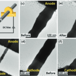
In this example, silver nanowires were placed on an E-chip (home-made) and exposed to a DC bias between both ends for in situ observation of electromigration. Material migration was observed after a slow biasing rate of 0.05 V min-1. The failure mechanism was believed to be caused not by heating, but by electromigration, which posed a greater risk of void formation, particularly in the presence of stacking faults.
Hsueh, Y. et al. (2023) ‘In Situ/Operando Studies for Reduced Eletromigration in Ag Nanowires with Stacking Faults’, Advanced Electronic Materials, p. 2201054. Available at: https://doi.org/10.1002/aelm.202201054.
With this workflow, scaling bulk electronic device experiments to the nanoscale becomes easier, while maintaining the highest level of scientific rigor to publish relevant, reproducible and reliable results.
Want to know more about electronic device research using in situ microscopy? Look up our one pager here!